Semiconductors
EDXRF / XRF for Semiconductors & Magnetic Media
Thickness and Elemental Composition of Multi-layer Thin Films
Semiconductor device fabrication is the process used to create the integrated circuits (silicon chips) present in everyday electrical and electronic devices. It is a multiple-step sequence of photographic and chemical processing steps during which electronic circuits are gradually created on a wafer made of pure semiconducting material. Silicon is the most commonly used semiconductor material today, along with various compound semiconductors. From start to packaged chips ready for shipment, the entire manufacturing process takes six to eight weeks and is performed in a highly specialized facility known as a FAB.
Magnetic memory is an engineering term referring to the storage of computer, audio, or video data and is a form of non-volatile memory. Information is typically accessed using one or more read/write heads.

Thickness & Composition without Standards
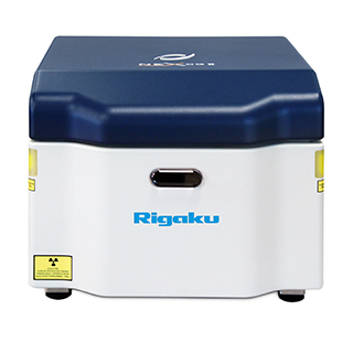
The NEX CG II Series benchtop spectrometers are powered by Rigaku’s RPF-SQX Fundamental Parameters (FP) software, featuring Rigaku Profile Fitting (RPF) technology and Scattering FP. This robust software allows semi-quantitative analysis of almost all sample types without standards – and rigorous quantitative analysis with standards.
The layer thickness and chemical composition of multi-layer samples are easily determined with energy dispersive X-ray fluorescence analysis (EDXRF) — for thin films down to several atomic layers (less than 1 nm) and up to the µm or even mm-range. Using Rigaku RPF-SQX FP approach may be employed for all calculations, and without the use of standards (i.e., no specific multi-layer standards are required). Nevertheless, any available multi-layer standard can be used to optimize the results.
Semiconductor Information & Resources

